
In the ever-evolving world of technology, much attention is given to the final products—smartphones, laptops, solar panels, and medical devices. However, at the core of all these systems lies a seemingly simple but incredibly sophisticated material: silicon . More specifically, silicon wafers and silicon substrates form the basis upon which most modern electronic components are built. This article explores the significance, structure, manufacturing processes, and applications of silicon wafers and substrates. Whether you’re a student, engineer, or simply curious about the science powering modern electronics, this guide will offer a detailed, structured look into these essential materials.
Table of Contents
-
- Introduction to Silicon
-
- What Are Silicon Wafers?
-
- What Are Silicon Substrates?
-
- Key Differences: Wafers vs. Substrates
-
- How Silicon Wafers Are Made
-
- Applications in Modern Technology
-
- Material Properties of Silicon
-
- Industry Challenges and Future Directions
-
- Conclusion
Introduction to Silicon
Silicon is the second most abundant element in the Earth’s crust, found predominantly in the form of silicon dioxide (SiO₂). Despite its natural abundance, the silicon used in the semiconductor industry must undergo extensive purification to achieve the electrical properties necessary for microelectronics. The widespread use of silicon in electronics is due to its excellent semiconducting properties, cost-effectiveness, and well-established manufacturing infrastructure.
What Are Silicon Wafers?
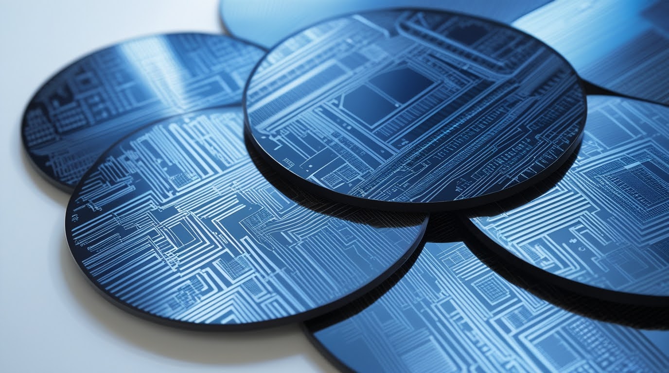
A silicon wafer is a thin, flat disc of semiconductor-grade silicon used as the foundational platform for manufacturing microelectronic devices. These wafers are sliced from a single-crystal silicon ingot and processed to create a clean, flat, and defect-free surface suitable for photolithography, doping, and circuit patterning.  To learn more about wafer specifications and availability, see silicon wafers . Key Characteristics of Silicon Wafers:
-
- Diameter: Common sizes include 100 mm, 150 mm, 200 mm, and 300 mm.
-
- Thickness: Varies with diameter; generally between 200 µm to 800 µm.
-
- Crystal Orientation: Typically (100), (110), or (111).
-
- Doping: Includes p-type or n-type using dopants such as boron, phosphorus, or arsenic.
What Are Silicon Substrates?
The term silicon substrate refers to any silicon-based material that acts as a base layer for device fabrication. While all silicon wafers are substrates, not all substrates are classified as wafers. Substrates may be used for epitaxial growth, MEMS devices, and research platforms, and they come in a variety of shapes and levels of processing. Silicon substrates may include:
-
- Bulk monocrystalline silicon
-
- Silicon-on-insulator (SOI) substrates
-
- Porous silicon
-
- Silicon carbide and compound semiconductors (in extended definitions)
They serve as the structural and functional foundation for depositing, etching, or growing other semiconductor layers and devices.
Key Differences: Wafers vs. Substrates
Though closely related, silicon wafers and silicon substrates serve slightly different roles depending on context. Here’s a breakdown:
| Feature | Silicon Wafer | Silicon Substrate |
| Shape | Always circular, thin, and polished | Can be circular, square, or custom-shaped |
| Primary Use | Fabrication of integrated circuits | Broad applications: epitaxy, MEMS, research |
| Manufacturing Stage | Finalized, ready for device layering | May be pre-processed or raw |
| Orientation Control | Strictly defined (e.g., (100), (111)) | May vary depending on application |
| Industry Context | IC fabrication, solar cells | Broader: also includes sensors, LEDs, R&D |
How Silicon Wafers Are Made
 The production of high-quality silicon wafers involves multiple precision-engineered steps to ensure optimal electrical and physical properties. Here is a simplified overview:
1. Purification of Silicon
-
- Quartz (SiO₂) is reduced with carbon in electric furnaces to create metallurgical-grade silicon.
-
- Further purification via the Siemens process yields electronic-grade silicon with 99.9999% purity.
2. Crystal Growth
-
- Czochralski (CZ) Process: A seed crystal is dipped into molten silicon and slowly pulled upward while rotating to form a cylindrical ingot of monocrystalline silicon.
3. Ingot Processing
-
- The silicon ingot is shaped and sliced into wafers using diamond wire saws.
-
- Edge rounding helps reduce wafer chipping.
4. Lapping and Etching
-
- Lapping removes saw marks.
-
- Chemical etching removes microscopic surface damage and contamination.
5. Polishing
-
- One or both sides are polished to achieve mirror-like flatness required for photolithography.
6. Doping (Optional)
-
- Doping alters electrical conductivity. P-type (boron) or N-type (phosphorus/arsenic) doping may be performed.
7. Final Cleaning and Inspection
-
- Cleanroom processes ensure particle-free, defect-free wafers.
-
- Wafers are then tested, sorted, and packaged.
Applications in Modern Technology
Silicon wafers and substrates are ubiquitous across many technological domains:
1. Integrated Circuits (ICs)
-
- Microprocessors
-
- Memory devices (RAM, Flash)
-
- Power devices
2. Photovoltaics
-
- Crystalline silicon solar cells (monocrystalline and polycrystalline)
-
- Emerging technologies using thin-film silicon
3. MEMS Devices
-
- Accelerometers
-
- Microfluidic sensors
-
- Pressure sensors
4. Optoelectronics
-
- Image sensors
-
- Photodetectors
-
- Light-emitting diodes (LEDs)
5. Quantum and Advanced Research
-
- Quantum computing prototypes
-
- Spintronic devices
-
- Nanofabrication research
Material Properties of Silicon
Silicon is chosen for wafer and substrate use because of a combination of favorable material properties:
| Property | Description |
| Semiconducting Bandgap | 1.12 eV – ideal for digital logic and switching |
| Thermal Conductivity | ~150 W/mK – helps dissipate heat in dense ICs |
| Hardness | Mohs scale of 7 – durable under fabrication stress |
| Crystal Structure | Diamond cubic – allows precise orientation control |
| Abundance | Earth’s crust contains ~28% silicon by weight |
These attributes make silicon not only abundant and affordable but also technologically optimal for semiconductor fabrication.
Industry Challenges and Future Directions
1. Miniaturization and Node Scaling
As the industry approaches sub-3 nm technology nodes, controlling defects, flatness, and doping profiles at atomic scales becomes increasingly difficult.
2. Material Limitations
While silicon works well for general-purpose semiconductors, it underperforms in high-frequency or high-power applications. This has led to interest in alternative substrates like GaN and SiC.
3. Integration of Heterogeneous Materials
Advanced packaging techniques are pushing the limits of how different materials—like III-V semiconductors and oxides—can be integrated on silicon substrates.
4. Environmental Impact
The wafer production process consumes significant energy and chemicals. Innovations in reclaiming and recycling wafers aim to make production more sustainable.
5. Silicon Photonics
Research is ongoing into integrating optical communication channels within silicon chips to enhance speed and efficiency, particularly in data centers.
Conclusion
From the computer on your desk to the solar panel on your roof, silicon wafers and silicon substrates underpin nearly every modern electronic device. Understanding how these materials are made and used provides valuable insight into the structure and future of technology. While silicon remains the workhorse of the semiconductor industry, continuous innovation is essential to meet the growing demands of smaller, faster, and more efficient devices. As we move toward an era of quantum computing, AI, and advanced communications, the role of foundational materials like silicon will continue to evolve. A deep understanding of these materials helps inform better engineering decisions and more sustainable manufacturing practices.