
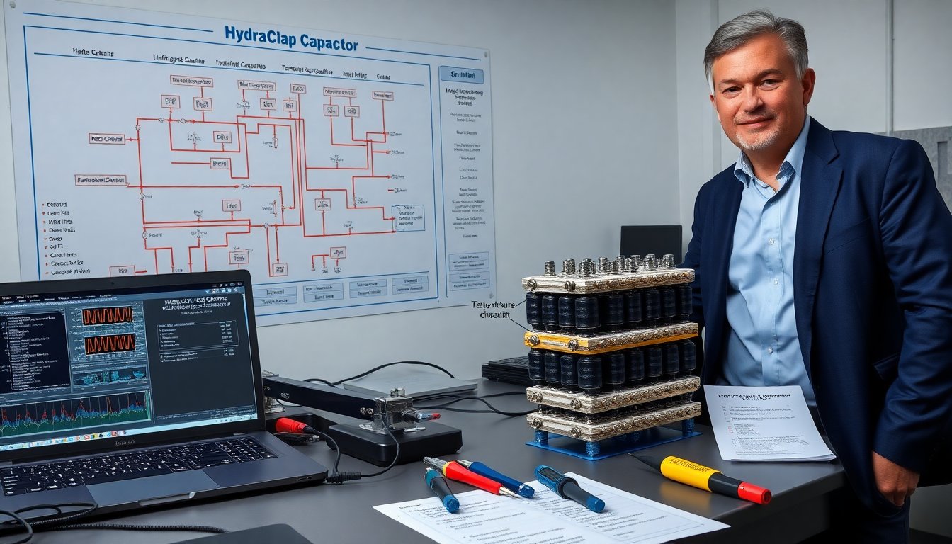
HydraClap capacitor duros tech schematics appear here as a focused guide. It explains what the module does and why Duros Tech chose this approach. The text shows core parts, signal paths, and reading tips. The tone stays technical and clear. The guide assumes basic electronics knowledge and gives practical steps for engineers and technicians.
Key Takeaways
- The HydraClap capacitor duros tech schematics describe a hybrid energy-storage module designed for fast charge release and long service life by pairing high-density films with a low-impedance bus and active balancing.
- Duros Tech’s capacitor architecture uses stacked metallized polypropylene film cells with an active balancing board employing MOSFETs and a microcontroller to maintain voltage balance and protect the stack via thermal and overvoltage circuits.
- The schematics include detailed circuit blocks, signal flow, and key symbols, highlighting components like the cell array, balancing board, protection stage, and monitoring bus for clear understanding and troubleshooting.
- Technicians use marked test points TP1 through TP12 to measure cell voltages and diagnose faults, following safety protocols such as controlled discharge and PPE use due to stored lethal energy.
- The design targets applications needing burst power and frequent cycling, such as grid support and regenerative braking, with documentation supporting impedance matching, cooling, and safe repair with assembly torque specifications and fault voltage tables.
What The HydraClap Capacitor Is And Why Duros Tech Uses This Architecture
The HydraClap capacitor duros tech schematics describe a hybrid energy-storage module. Duros Tech designed the module to provide fast charge release and long service life. The module pairs high-density films with a low-impedance bus and active balancing. The design reduces ripple and extends cycle count. Engineers at Duros Tech chose this architecture to meet peak discharge and tight space limits.
The block offers three main functions. First, it stores charge across stacked capacitor cells. Second, it controls cell voltage with an active balancing board. Third, it protects the stack with thermal and overvoltage circuits. The stack uses metallized polypropylene films for low loss and long life. The balancing board uses MOSFET switches and a small microcontroller to move current between cells.
Designers placed the bus bars to keep series inductance low. They placed test points near cell pairs to ease measurement. They used paralleled low-ESR capacitors where high current pulses occur. The layout reduces hot spots and helps cooling. The overall result shows high pulse capability with predictable aging. Technicians read the schematics to plan repairs and to check compatibility with inverters and converters.
This module targets applications that need burst power and frequent cycling. Examples include grid support, regenerative braking, and pulse lasers. Duros Tech published the schematics to help integrators match impedance and cooling. The published files show connector pinouts, PCB layers, and shielding details. The files also list tolerances and assembly notes for critical joints.
Detailed Schematic Walkthrough: Circuit Blocks, Signal Flow, And Key Symbols
The HydraClap capacitor duros tech schematics split the design into five circuit blocks. The blocks show the cell array, balancing board, protection stage, charge interface, and monitoring bus. The schematic uses clear symbols for capacitors, switches, thermistors, and connectors. The signal flow moves from the charge interface to the cell array and then to the protection stage on discharge.
The charge interface uses a current-limited input with an EMI filter. The schematic shows input fuses and surge suppression. The cell array uses series stacks with interleaved parallel legs. The schematic marks each cell with an ID number and capacitance value. The balancing board connects to each cell via sense lines. The board shows MOSFETs placed in a H-bridge style for charge transfer. The software on the balancing MCU measures voltage and opens or closes MOSFETs to equalize cells.
The protection stage sits between the cell array and the output. The stage uses contactors and a crowbar MOSFET. The schematic lists trigger thresholds and hysteresis values. The stage also shows a thermal cutout triggered by temperature sensors mounted on the bus bars. The monitoring bus uses an isolated CAN interface. The schematic clarifies pin assignments and termination resistors.
Duros Tech marks test points and measurement nodes on the schematic. The designer places TP1 through TP12 at cell junctions. The schematic shows recommended probe ground points and expected voltage ranges. The document includes a table of normal and fault voltages for quick checks. The schematic uses color-coded nets in the PDF to help visual scanning.
The legend lists symbol conventions. Capacitors use the standard parallel-plate symbol and a suffix to show film type. MOSFETs show gate, drain, and source with package codes. Connectors show mating face and pin numbers. The schematic includes an assembly note that specifies torque values for bus bar bolts and solder process windows for PCB-mounted parts.
Identifying Critical Components, Test Points, And Safe Troubleshooting Practices
Technicians find the HydraClap capacitor duros tech schematics useful for repairs. The schematic highlights three critical component groups: cell modules, balancing board, and protection stage. Technicians inspect these groups first during a failure. They check cell voltages, balance board signals, and protection triggers.
Technicians use the provided test points to isolate faults. They probe TP1 through TP12 to confirm cell voltages. They measure across the balancing board sense resistors to verify current flow. They check MOSFET gate voltages to confirm switching. They inspect contactor coil voltages when the system fails to energize.
The schematic also lists expected steady-state readings. For a healthy stack, each cell shows near-equal voltage within the tolerance band. The balancing board pulses small currents to adjust cells. If one cell falls outside the band, the schematic suggests replacing the affected cell pair. The document warns about mixing cells of different age or capacity.
Safety notes sit on the schematic front page. The notes warn that the module stores lethal energy after disconnect. The schematic instructs technicians to short the module through a controlled resistor before any hands-on work. The schematic lists the safe discharge path and required PPE. It also instructs technicians to isolate the CAN or control interface before powering the board.
For troubleshooting, the schematic recommends a stepwise check. First, confirm isolation and PPE. Second, measure cell voltages at test points. Third, check balancing MOSFET operation. Fourth, verify protection triggers and contactor control. Fifth, consult the assembly torque table if bus bar resistance looks high. The schematic includes a final checklist for reassembly and functional testing.

